Anonymous Verified Buyer
" Very responsive and helpful, competitive pricing. Good source! "
July 2025
USRP RF Daughterboard, 16 Digital I/O Lines, Ettus Research RF Module
Rated 4.5/5 | 11 ratings
Actual item may vary if no part number is provided on quote request.
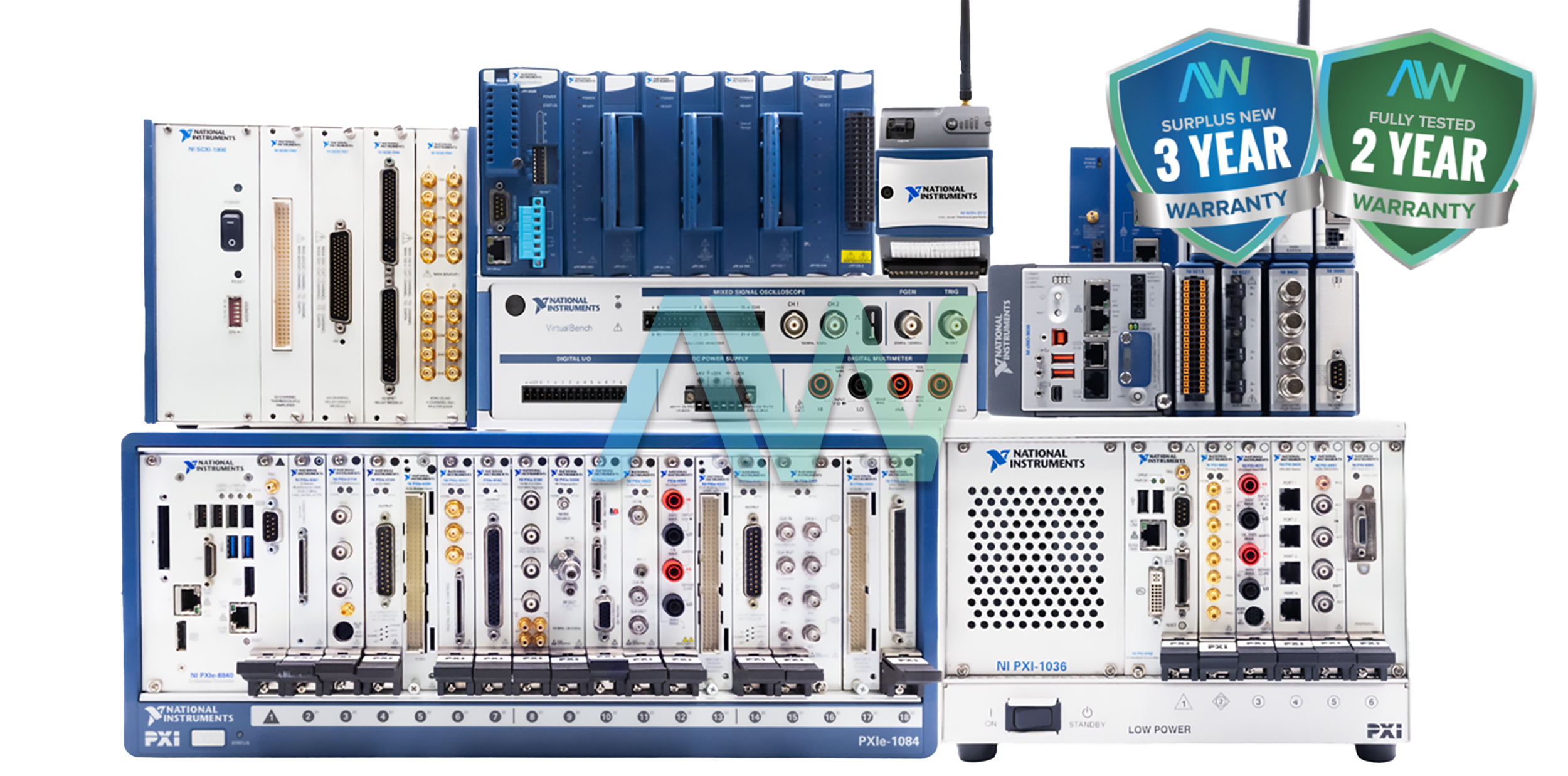
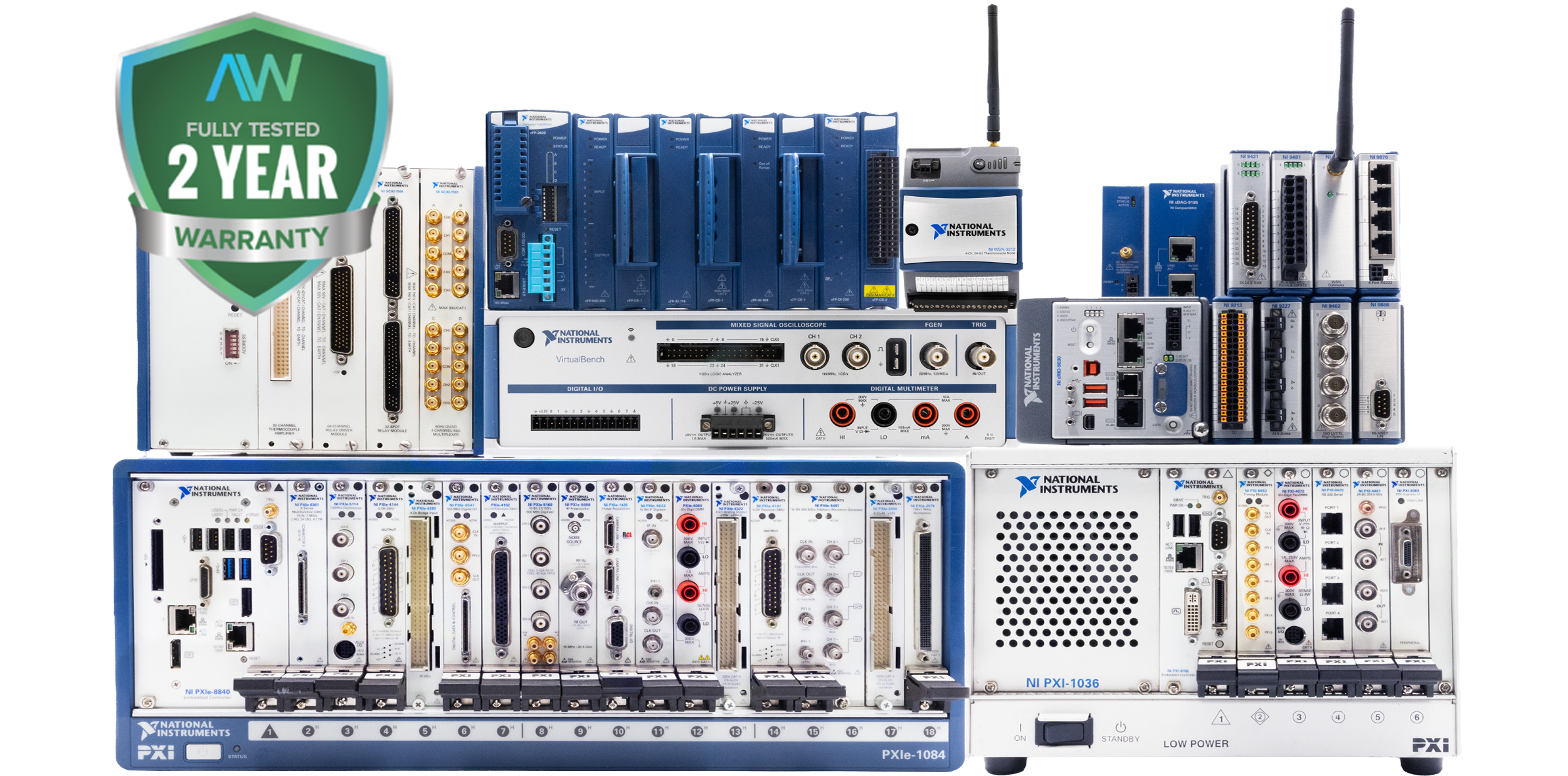
✔ 2 Year Warranty Included
✔ Free Ground Shipping
✔ NIST Calibration Available
Anonymous Verified Buyer
" Very responsive and helpful, competitive pricing. Good source! "
July 2025
Andrew Gar**** Verified Buyer
" Amazing to work with and had my order within 1 week after purchasing with all NI certs and data that were needed. "
March 2025
Said Sai**** Verified Buyer
" Competent contact for highly specialized components. The support team is very knowledgeable. Many thanks for the help and the fast shipping! "
January 2025
Bob C**** Verified Buyer
" Jason was able to get our emergency situation taken care of quickly and professionally. "
May 2025
Gregg Flecki**** Verified Buyer
" Great service and great products. This is my 2nd time using Apex Waves, truly impressed. "
January 2025
Carol Zimme**** Verified Buyer
" Very responsive and helpful, competitive pricing. Good source! "
July 2025
Andrew Gar**** Verified Buyer
" Amazing to work with and had my order within 1 week after purchasing with all NI certs and data that were needed. "
March 2025
Said Sai**** Verified Buyer
" Competent contact for highly specialized components. The support team is very knowledgeable. Many thanks for the help and the fast shipping! "
January 2025
Bob C**** Verified Buyer
" Jason was able to get our emergency situation taken care of quickly and professionally. "
May 2025
Gregg Flecki**** Verified Buyer
" Great service and great products. This is my 2nd time using Apex Waves, truly impressed. "
January 2025
National Instruments USRP RF Daughterboard
The USRP RF Daughterboard is a fully synchronous RF module designed for advanced MIMO applications. It supports complete I/Q architecture by enabling high-fidelity signal transmission and reception. The board operates in full-duplex mode. All transmit and receive functions can be controlled directly from software or FPGA. The daughterboard includes built-in T/R switching functionality which simplifies antenna configuration and system integration. Users can select to operate TX and RX on the same connector or utilize an auxiliary RX port. It provides 16 digital I/O lines for controlling external devices.
The transmit power and receiver gain are fully adjustable by providing precise control over signal levels. The PLL lock time of the board is less than 200 microseconds by enabling frequency hopping applications. It supports 30 megahertz transmit and receive bandwidth natively. The board interface exposes all signals including digital I/O, SPI and I2C buses, and low-speed ADCs and DACs. The developers can access all signals to create custom daughter-boards or FPGA designs. The XCVR2450 allows integration with advanced signal processing systems. It also contains Ethernet and dual one-gigabit connections. It includes a large user-programmable Kintex-7 FPGA for advanced digital processing.
The interface supports direct access to transmit and receive chains for full system visibility. Developers can integrate the board with other modules to create scalable testbeds. The board is compatible with advanced software-defined radio frameworks. Real-time control of all board functions is possible through software APIs or FPGA logic. The USRP RF board achieves low-latency operations suitable for frequency hopping and fast modulation schemes. Adjustable transmit power allows optimization for different communication standards. Receiver gain can be tuned to improve signal-to-noise ratio under varying conditions. The module is suitable for both laboratory research and field deployments requiring flexible radio frequency control.
The USRP RF Daughterboard enables development of custom signal processing pipelines with minimal latency. The high-speed digital input and output lines allow direct interaction with external circuits. The SPI and I2C protocol for buses provide additional configuration and control options for peripheral components. The unit contains low-speed analog and digital systems that provide essential feedback and monitoring capabilities.
| Model Name | USRP RF Daughterboard |
|---|---|
| Manufacturer | NI/Ettus Research |
| Part Type | Daughterboard |
| Architecture | Fully synchronous I/Q design |
| MIMO Capability | Supported |
| Digital I/O Lines | 16 lines for external device control |
| Adjustable Parameters | Transmit power and receiver gain |
| PLL Lock Time | < 200 µs |
| Bandwidth | 30 MHz native transmit/receive; daughterboard interface up to 40 MHz |
| Interface Access | 16-bit high-speed digital I/O, SPI, I2C, low-speed ADCs/DACs |
Associated part numbers for USRP RF Daughterboard:
Delivery:
No hassle return policy.
Dedicated customer service team.
Payment:


Receive Price & Availability Today!
Ask About Our Tiered Calibration Levels
Option & Modules:
Confirm Your Requirements or Versions
Cost & Lead Time Available Upon Request for Service
Repair Evaluation: $150
Common Typos: